Voltage Inverter Device
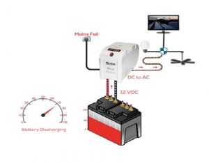
Generally, many people have confused on voltage inverter and converter, and their working principles. An inverter is an electrical device, which converts DC power to AC power and either increases or decreases the voltage level accordingly. In comparison, a converter changes the voltage level but does not change its type. So in converters, an AC voltage would still be AC and a DC voltage would still be in DC. Inverters are becoming more popular along with along with solar power systems where we get a low voltage DC supply to power ordinary appliances that either run on 110V or 220V AC.
Inverters are used in a large number of electrical power applications. Voltage inverters are divided into three categories, Pulse-width Modulated Inverters, Square-wave Inverters, and Single-phase Inverters with Voltage Cancellation.
Voltage Inverter Working Principle?
The basic idea behind every inverter circuit is to produce oscillations using the given DC and apply these oscillations across the primary of the transformer by amplifying the current. This primary voltage is then stepped up to a higher voltage depending upon the number of turns in primary and secondary coils.
Most inverters are of the variable voltage, variable frequency design. They consist of a converter section, a bus capacitor section and an inverting section. The converter section uses semiconductor devices to rectify (convert) the incoming fixed voltage, fixed frequency 3-phase AC power to DC voltage which is stored in the bus capacitor bank.
There it becomes a steady source of current for the power devices which are located in what is known as the inverting section. The inverting section absorbs power from the DC bus cap bank, inverts it back to simulated 3-Phase AC sine waves of varying voltage and varying frequency that are typically used to vary the speed of a 3-phase induction motor.

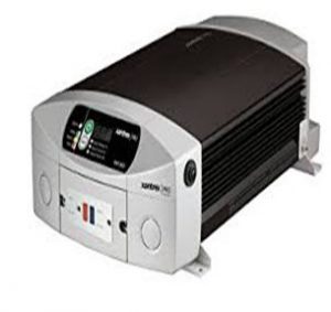
Voltage Inverter
Steps to Make a Voltage Inverter Circuit
The different steps to make a voltage inverter includes the following
Required Components
- Breadboard to place all the components and to solder everything on
- LM555IC chip is the heart of the circuit
- The values of Resistors, capacitors, and diodes are shown in the circuit below.
- Color LEDs and voltage supply
Add the IC LM555 Chip
- Place the LM555IC chip on the breadboard which is the heart of the entire circuit
- Give the voltage supply and GND
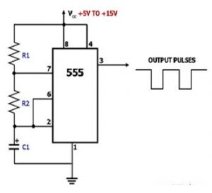
- Connect the two pins from Pin 6 to Pin 2 and connect the two resistors R1, R2
- Add a Capacitor C1
- Watch out of the Positive and the Negative connections of the capacitor
- The LED has two terminals namely positive and negative, where a shorter leg is the negative terminal

IC LM555 Chip Pulse Generator
Design the Circuit by Connecting the Components
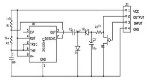
The voltage inverter circuit is shown below, that uses a well known LM555IC timer chip. The schematic diagram divided into three parts, namely an oscillator, rectifier, and voltage regulator.An oscillator is used to convert DC into AC, a special type of rectifier is used to convert AC to DC and finally a voltage regulator.

Voltage Inverter Circuit
- An oscillator is used to convert DC into AC, a special type of rectifier is used to convert AC to DC and finally a voltage regulator.
- This IC in the above circuit is wired as an oscillator. The high period of the of the cycle acquires 0.6933× (R1+R2) ×C1 Secs and the low period acquires 0.693×R2×C1 Sec.With the R1, R2 and C1 values, this generates a square wave approximately 1.3 kHz at pin-3.
- The connection of the two diodes provides rectification and certainly, they do generate a DC signal, but in a dissimilar way than the general diode bridges.
- When pin-3 of the IC is high, the D1 diode ON and conducts and thus the IC charges C2 capacitor. When pin-3 toggles low, the diode D1 OFF and it blocks current.
- There will be a charge of C2 capacitor and the positive side of the capacitor is now the 0V level. The other side must then be -VCC if we neglect the threshold of D1 diode for a while.
- That means that diode D2 performs and capacitor C2 charges, C3 with a -Ve voltage. And capacitor C3 works as a smoothing capacitor.
- That means that diode D2 performs and capacitor C2 charges, C3 with a -Ve voltage. And capacitor C3 works as a smoothing capacitor.
- As said, the o/p stress must be controllable. The best way to do is to make a changeable voltage divider with one variable resistor and a fixed resistor. This is the merge of R3 & Q1 here, Q1 is a P-channel junction field effect transistor.
- Before turning up this circuit, you can try to use the voltage control as Vcc, and go down R3 and Q1.Though, the H0420 design, the pin of the LC-driving voltage couldn’t produce an ample current to feed the IC chip.
- In addition, this IC requires a power supply of 4.5V. There are other implementations of the IC. A low-power CMOS version of the chip would obey the power supply of the LC-driving voltage pin of the H0420. low-power CMOS version of the chip would obey the power supply of the LC-driving voltage pin of the H0420.
Applications of voltage inverter
Inverters are a practical device and are a useful piece of equipment for many different applications. Anyone who wants to run a laptop or other electronic device within a car or RV an inverter is required.
Different inverters may have different features making them better suited for different specific applications. Very small inverters are available that connect to a car cigarette lighter, with a single three-prong AC outlet as the output.
Large inverters are generally designed to be hardwired into a building electrical system. Some inverters offer 240 volts output.
Inverter types can be categorized by output waveform, switch type, switching technology and frequency.
Know more about Three Phase Inverter.
know more about Single Phase Inverter MCQs, Toggle Switch MCQs..
Thus, this is all about steps to make a voltage inverter circuit. Furthermore, any queries regarding this concept or electrical and electronics projects, please give your valuable suggestions by commenting in the comment section below. Here is a question for you, what is the main function of an inverter?