An amplifier is an electronic circuit that is used to amplify the voltage signal or a current signal. The amplifier circuits are generally designed with one or more transistors. A BJT or a FET transistor is a major component of the amplifier system. They can be categorized into a weak signal amplifier or a power signal amplifier and are used in wireless communication and broadcasting, and audio equipment. This article discusses the common collector amplifier which is the amplifier topologies.
What is Common Collector Amplifier
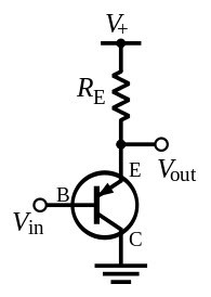
The common collector amplifier is one of the three basic BJT amplifier topologies. In this circuit, the base of the transistor serves as an input, emitter as the output and the collector is grounded that is, common for both emitter and base. It is also called as an emitter follower. This configuration acts as a buffer. This circuit provides offer low output impedance while taking high input impedance. This configuration is mainly used in digital circuits with logic gates and has many applications.
Common Collector Configuration
Characteristics of Common Collector Amplifier
The load resistor in the common collector amplifier being placed in series with the emitter circuit receives both the base current and collector currents.
Since the emitter of a transistor is the sum of the base and collector currents, since the base and collector currents always add together to form the emitter current, it would be reasonable to assume that this amplifier will have a very large current gain.
The common collector amplifier has quite a large current gain, larger than any other transistor amplifier configuration. The characteristics of the common collector amplifier as mentioned below.
| Parameter | Characteristics |
| Voltage gain | Zero |
| Current gain | High |
| Power gain | Medium |
| Input or output phase relationship | Zero degree |
| Input resistance | High |
| Output resistance | Low |
Input Characteristics
The common collector characteristics are quite different from the common base and common emitter characteristics. This is because the input voltage Vbc is largely determined by the output voltage Vec. As Vbc increases with Vec constant Veb decreases hence Ib decreases.
Common Collector Configuration
Output Characteristics
Here as Vcc increases Ie also increases. Just as in common emitter output characteristics Ic increases with increasing Ib, so Ie also increases here with the increase in Ib. Hence, for constant Vec, Ie increases with Ib.
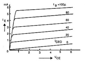
Output Characteristics of Common Collector
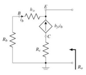
The small signal circuit performance can now be calculated. Total circuit performance is the sum of quiescent and small signal performance. The AC model circuit is shown below.
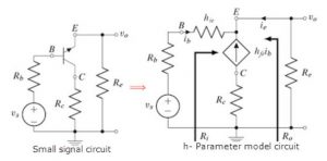
AC Modeling of Common Collector Amplifier
Current Gain
The current gain is defined as the ratio of the load current to the input current.
Ai= il/ib= -ie/ib
From the h-parameter circuit, it can be determined that the emitter and base currents are related to the dependent current source by the constant hfe+1. The current gain is dependent only on the BJT characteristics and independent of any other circuit element values. Its value is given by
Ai= hfe+1
Input Resistance
The input resistance is given by
![]()
![]()
This result is identical to that for a common emitter amplifier with an emitter resistor. The input resistance to a common collector amplifier is large for typical values of the load resistance Re.
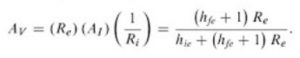
Voltage Gain
The voltage gain is the ratio of output voltage to input voltage. If the input voltage is again taken to be the voltage at the input to the transistor, Vb.
Av= Vo/Vb
Av= (vo/il)(il/ib)(ib/vb)
Replacing each term with its equivalent expression
Av= (Re)(Ai)(1/Ri)
The above equation is somewhat less than unity. The approximation equation of voltage gain is given by
The overall voltage gain can be defined as
Avs= Vo/Vs
This ratio can be directly derived from the voltage gain Av, and a voltage division between the source resistance Rs and the amplifier input resistance R.
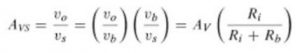
After substitutions of appropriate equations, the overall voltage gain is given by
Avs= 1- (hie+Rb) / (Ri+Rb)
Output Resistance
The output resistance is defined as the Thevenin resistance at the output of the amplifier looking back into the amplifier. The circuit is shown below, the AC equivalent circuit to calculate the output resistance.
Common Collector Output Resistance AC Equivalent Circuit
If a voltage v is applied to the output terminals, the base current is found to be
ib= -v/(Rb+hie)
The total current flowing into the BJT is given by
i= -ib – hfe . ib
The output resistance is calculated as
Ro= v/i = (Rb+hie) / (hfe+1)
The output resistance for a common collector transistor amplifier is typically small.
Applications
- It is useful as an impedance matching device since its input impedance is much higher than its output impedance.
- It is used in digital circuits with logic gates.
- It is used as a switching circuit.
- It is also used for cascade amplifier circuit isolation.
This article discusses the working of the common emitter amplifier circuit and its applications. By reading the above information you have got an idea about this concept. Furthermore, any queries regarding this article or if you want to implement Electrical and Electronic projects please feel free to comment in the below section.