An operational amplifier which is termed a high gain, DC coupled, inverting feedback amplifier was initially observed in the year 1941 by Karl D. Swartzel. In this configuration, the amplifier is designed using three vacuum tubes which results in a gain of 90 dB, and it functions in the voltage range of ±350 volts. This operational amplifier was just a single inverting type of amplifier and does not have differential inverting and non-inverting inputs. Whereas, the initial explicit non-inverting type of amplifier was invented in 1947 by John R. Ragazzini. Later on, there were many advancements in the design and versions of the device. Now, this article focuses on explaining non inverting op amp definition, working, circuit, types, applications and uses.
What is Non Inverting Op Amp?
A non inverting operational amplifier is termed as op-amp which delivers an amplified output and this output is exactly in the same phase as the provided input signal. This circuit performs like a voltage follower circuit which works with a negative feedback connection, but only some portion of the output signal is provided as feedback to the inverting input terminal of the operational amplifier.
For this circuit, when the input and output impedance levels are high and low correspondingly, then the device is perfect for many impedance buffering applications.
The non inverting op amp waveform for input and output signals is shown below:
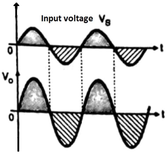
Output Waveforms
The signal that has to be amplified is provided as input to the positive node (non inverting node) of the operational amplifier whereas the negative node (inverting node) is ground-connected using Ra resistor. The voltage values of input and output waveforms are exactly in phase with each other so that the phase difference is 00.
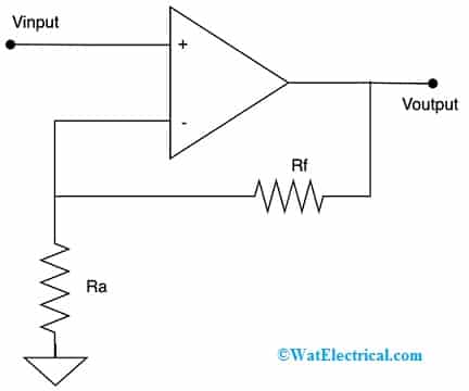
Circuit Diagram of Ampliier
When any signal is applied to the non inverting node, the polarity of the applied signal is not changed at the output but only gets amplified. This shows the amplifier gain as positive.
With the above theory, when the amplifier gain is positive, then the positive sign indicates that there exists no phase shift between the input and output signals, and the voltage gain is based on Ra and Rf resistors. When the values of Ra and Rf are adjusted, then necessary gain can be achieved.
Non Inverting Op Amp Derivation
Below is the non inverting op amp circuit diagram having a feedback loop.
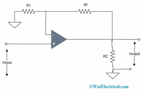
Non-Inverting-Op-Amp
Non Inverting Op Amp
As per the above circuit, to the inverting input external resistor (R1) and feedback resistor (Rf) are connected. When we apply KCL principle to the inverting input, then
V1/R1 = (V0– V1)/Rf
Consider that the voltage at the non inverting terminal is Vi. At this condition, when the operational amplifier is considered to be in ideal condition, then V1 = Vi
So the above inverting input equation is written as
Vinput/R1 = (V0utput– Vinput)/Rf
- ð Vinput (Rf/Ri) = Vinput – Vinput
- ð V0utput/Vinput = (1 + Rf/Ri)
This is the feedback voltage formula at R1.
So, the gain of non inverting amplifier formula for closed-loop condition is
A = Voutput/Vinput
A = (1 + Rf/Ri)
The gain of the circuit does not consist of any negative components which indicate that the input signal is amplified at the output having no change in the polarity.
Virtual Short in Non Inverting Op Amp
In a non inverting op amp, there is the condition of virtual short in between the input pins. The virtual short is termed an open circuit for the current and a short circuit for voltage. In the virtual short condition, two features of ideal op amp are used which are:
- As Ri approaches infinity, the input current will be ‘0’ at both terminals.
- As the gain of the open loop is infinite, the difference between V1 and V2 will be ‘0’.
Also, the gain of non inverting op amp appears ‘0’, when Rf equals to ‘0’ or R1 approaches infinity.
A = (1 + Rf/Ri)
- ð (1 + 0/Ri)
- ð A = 1
When R1 approaches infinity, then
A = (1 + Rf/∞)
A = 1
So, when the feedback path is short-circuited or the external resistance for the inverting input is opened, then non inverting op amp gain becomes ‘1’.
During the virtual short condition, it delivers exact results when it is operated in heavy negative feedback scenarios. The voltage gain in the open loop condition will be infinity until the op amp functions in the linear region.
In this virtual short state, the voltage at inverting input is the same as the voltage at non inverting input which means that when the inverting input voltage rises or falls, the same happens at non inverting input voltage. This condition is termed as Bootstrapping.
Input and Output Impedance
The input impedance formula for non inverting operational amplifier is given by
ZInput = (1 + AOLβ) Zi
Here, ‘AOL’ corresponds to the gain in the open loop condition
‘Zi’ corresponds to input impedance when no feedback is connected
‘β’ corresponds to the feedback factor
In the non inverting op amp, ‘β’ = R2/ (R1 + R2)
β = 1/A
So, input impedance is
ZInput = (1 + (AOL/A) Zi
The output impedance is
ZOutput = Z0/ (1 + AOLβ)
As β = 1/A
ZOutput = Z0/ (1 + (AOL/A))
Types
There are few non inverting op amp types which are explained as below:
Single Supply Non Inverting Op Amp
In general, operational amplifiers are constructed with two power supplies which can be +10V and -10V. In making the design easy, a single supply op amp is used where the single supply configuration can be achieved by half supply railing which corresponds that the circuit is biased to the half of rail voltage. When the functional point is set to this rail voltage, the maximum value of the swing can be achieved at the output. The below diagram shows the circuit of a single supply non inverting op amp.
While operating this circuit, the below points have to be considered.
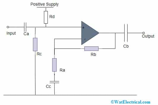
Non-Inverting Op Amp with Single Supply
Single Supply Non Inverting Op Amp
- 1. Input Impedance – When compared with a general operation amplifier, this configuration offers minimal impedance. Here, the input impedance is given by
(Rc * Rd) / (Rc + Rd)
- Input and Output Capacitance values – While designing any electronic circuit, the values of input and output capacitors are selected in a way so that minimal frequency levels are passed having no undue attenuation.
- Bias Voltage – For this single supply non inverting op amp, the bias voltage value is set to half the value of rail voltage. With this, the output can be enabled so that it has a similar swing in both directions having no clippage.
- Capacitor Cc– The leakage from Cc should be very minimal if not the leakage current shows trouble to the circuit. Electrolytic capacitors do not operate in this position as because the leakage current values are high.
AC Coupled Non Inverting Op Amp
In many scenarios, we observe that circuits are DC couples. While connecting the circuit in AC coupled mode, it has to be made sure that the op amp should have a DC path to ground for minimal values of input current. This is required for biasing the input device internal to the IC.
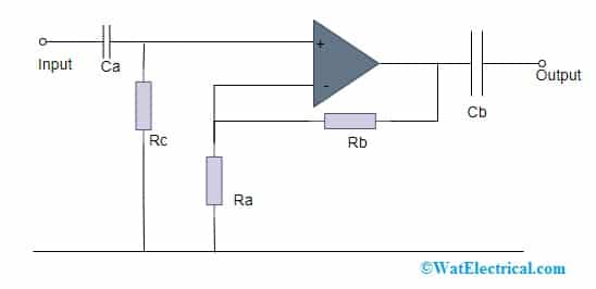
AC Coupled Op Amp
The AC coupling can be obtained by including a resistor (Rc) of high value and it is connected to the ground. This high value resistor ranges above 100kΩ. When this Rc is not included in the circuit, then the output of AC coupled non inverting op amp will drive into any one of the voltage rails.
When placing the Rc resistor in this approach, it has to be noted that capacitor and resistor (C1/Rc) forms HPF and this HPF does not have cut-off frequencies. The cut-off value appears at the frequency level where the resistance value equals capacitive reactance.
In the same way, the capacitor at the output has to be selected in the way to pass the minimal frequency levels required for the circuit. Here, the op amp’s output impedance reaches low and so the high impedance is probably the same as the next stage.
Summing Amplifier
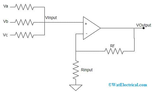
In the non inverting summing operating amplifier, the input voltages are fed to the non inverting input of the amplifier and some portion of the output is connected to inverting input terminal using the configuration of the voltage divider bias feedback loop. Here, any number of inputs can be added to the amplifier’s input. The circuit is shown as follows considering three inputs:
Summing Amplifier
To calculate the output voltage, the circuit has to be divided into two parts
- Source section
- Non inverting amplifier section
VInput is considered as the sum of all inputs (Va, Vb, and Vc) and then provided as input to the non inverting terminal of the amplifier. Rf and Ra are the feedback divider resistors.
Voutput = Vinput (1 + (Rf/Rin))
Using VOutput, VInput has to be known, when Va, Vb, and Vc are the three input supplies, then Ra, Rb, and Rc are the corresponding voltage values. So, VInput1, VInput2, VInput3 are the input sources of corresponding channels when the other channels are connected to ground. Then
VInput = VInput1 + VInput2 + VInput3
In the summing amplifier, there exists no virtual ground theory, so every channel shows impact on other channel. Now, VInput1 (which is a portion of VInput) is calculated and then the other two values VInput2 and VInput3 are easily calculated.
To know VInput1, Vb and Vc are connected to ground whereas their respective resistors are considered as they create a voltage divider network. So,
VInput1 = Va [Rb || Rc) / (Ra + (Rb || Rc))]
In the same way, VInput2 and VInput 3 are derived
VInput2 = Vb [Ra || Rc) / (Rb + (Ra || Rc))]
VInput3 = Vc [Ra || Rb) / (Rc + (Ra || Rb))]
Therefore,
VInput = Va [Rb || Rc) / (Ra + (Rb || Rc))] + Vb [Ra || Rc) / (Rb + (Ra || Rc))] + Vc [Ra || Rb) / (Rc + (Ra || Rb))]
Then VOutput = (1 + (Rf/ Rin)) { Va [Rb || Rc) / (Ra + (Rb || Rc))] + Vb [Ra || Rc) / (Rb + (Ra || Rc))] + Vc [Ra || Rb) / (Rc + (Ra || Rb))]}
When all the resistors are of same value, then the output voltage is represented as:
VOutput = (1 + (Rf/Rin)) (Va + Vb + Vc)/3)
So, non inverting summing amplifier is designed from the non inverting operational amplifier to provide the necessary voltage gain. Then the input values of resistors are chosen to be maximum so that that ensemble with the type of operational amplifier used.
Non Inverting Op Amp Problems
In the below circuit, find the values of amplifier gain, output voltage and current, and amount of current flow through the output resistor.
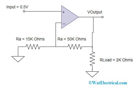
Example Problem
In the provided circuit, node A is considered non inverting, and node B is the inverting terminal which is the voltage follower circuit of the op amp.
The node B potential is VInput and due to virtual short condition,
Va = VInput = Vb = 0.5V
The current flow through I1 is
Ia = Va/Ra = 0.5V/15 KΩ
Ia = 30 µAmp
As the input current is ‘0’, the similar Ia should flow across Rf resistor.
Gain = A = 1 + (Rf/Ra)
- ð 1 + (50 KΩ/10KΩ)
So, gain A = 6
Output voltage , VOutput = Gain * Input voltage
VOutput = A * VInput
- ð 6 * 0.5V
- ð VOutput = 3V
The current flow through load resistor is given by:
ILoad = VOutput/RLoad
- ð 3V / (5 * 103Ω)
- ð ILoad = 6 mAmps
The current flow at output is
IOuput = I1 + ILoad
- ð 30 µAmp + 6 mAmps
IOuput = 6.03 µAmp
Differences between Inverting and Non-Inverting Operational Amplifier
The few differences to be observed between inverting and non inverting operational amplifiers are explained as follows:
| Inverting Op Amp | Non Inverting Op Amp |
| Here, the amplified output is out of phase of the input signal which is 1800 out of phase | Here, the amplified output is in phase with the input signal |
| The inverting terminal is ground connected | The non inverting terminal is ground-connected using a resistor |
| The gain is A = -(Rf/Ra), which is the ratio of resistance | The gain is A = 1 + (Rf/Ra), which is the ratio of resistance added with ‘1’ |
| The gain value is either > or < or = 1 | The gain value is always > 1 |
| The input impedance is the same as Ra resistance | The input resistance is high |
| The feedback loop used is of voltage shunt | The feedback loop used here is of voltage series |
What Is Non-Inverting Buffer?
A non inverting buffer is just a single-sourced digital buffer that reads the input value and delivers output.
What Is The Purpose Of An Inverting Op-Amp?
Inverting operational amplifiers are employed as they provide linear characteristics and also they are employed in the conversions of input current to the output voltage.
Why we Use IC 741?
It can deliver maximum voltage gains and also it can be used in achieving a wide range of voltage levels.
What Is the Difference Between Transistor And Amplifier?
The amplifier is used for the amplification of signal whereas a transistor is an electronic device that is used in designing an amplifier.
Which Transistor Is Used As Amplifier?
In most cases, an NPN transistor is used in designing an amplifier.
Advantages and Disadvantages
The advantages of non inverting op amp are:
- The output signals are amplified signals without having a change in phase.
- The voltage gain is high, positive, and changeable also.
- Non inverting op amp configuration is employed in multiple electronic circuits.
- One can achieve exact impedance matching
- When compared with other operational amplifiers, non inverting op amp delivers high input impedance.
- The gain is always > 1
The disadvantages of non inverting op amp are:
- Reduced stability than inverting op amp.
- When a high gain is required, a more number of stages gets added to the circuit thus increasing the circuit complexity.
Non Inverting Op Amp Applications
The non inverting op amp applications are:
- These operational amplifiers are employed in high impedance applications.
- Used in applications to execute mathematical calculations such as adder circuits.
- Employed in the isolation of specific cascaded circuits.
- Used as voltage follower circuit.
- Selective inversion circuits.
- Also the non inverting op amp’s are used as current to voltage converters and active rectifiers.
So, this is the whole concept of non inverting operational amplifier. The article helps us in providing information on non inverting op-amp circuits, types, example problems, uses, and advantages. Here is a question for you, what is an amplifier?