Power MOSFET
The Power MOSFET is a type of MOSFET. The operating principle of power MOSFET is similar to the general MOSFET. The power MOSFETS are very special to handle the high level of powers. It shows the high switching speed and by comparing with the normal MOSFET, the power MOSFET will work better. The power MOSFETs is widely used in the n-channel enhancement mode, p-channel enhancement mode, and in the nature of n-channel depletion mode. Here we have explained about the N-channel power MOSFET. The design of power MOSFET was made by using the CMOS technology and also used for development of manufacturing the integrated circuits in the 1970s.
What is a Power MOSFET?
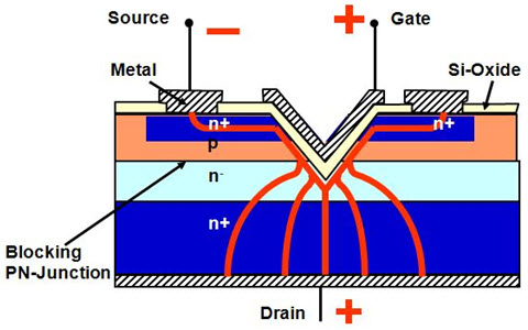
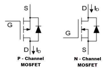
A power MOSFET is a special type of metal oxide semiconductor field effect transistor. It is specially designed to handle high-level powers. The power MOSFET’s are constructed in a V configuration. Therefore, it is also called as V-MOSFET, VFET. The symbols of N- channel & P- channel power MOSFET are shown in the below figure.
Basic Status of Power MOSFET
There is three basic status in the power MOSFET which is following.
- On sate resistance
- Breakdown voltage
- Body diode
On State Resistance
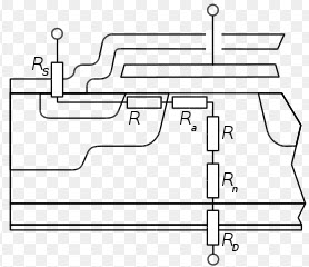
If the power MOSFET is in ON sate, then it produces the resistive behavior in-between the drain & source terminals. We can see in the following figure, that the resistance is the sum of many elementary contributions. The RS resistance is the source resistance. It will show all resistance between the source terminals of the package to the channel of the MOSFET.
On State Resistance
The Rch resistance is the channel resistance and this resistance is inversely proportional to the channel width & for a given die size, to the channel density. This resistance is very important contributors to the RDSon of the low voltage MOSFET. The intensive work has done to reduce their cell size with respect to increase the channel density.
The access resistance is represented by the Ra. The access resistance shows the resistance of the epitaxial zone directly to the gate electrode. The current direction is changed from the channel to the vertical.
RJFET is the detrimental effect of the cell size reduction. The P implantation is observed from the gate of a parasitic JFET transistor and it has reduced the width of the current flow.
Rn represents the epitaxial layer and it is used for sustaining the blocking voltage. This resistance is directly related to the voltage rating of the device. The high voltage MOSFET requires a thick low dependent layer which is highly resistive and a low voltage transistor requires a thin layer with the higher doping layer which is very less resistive. This is the main factor for the resistance of high voltage MOSFET.
The RD resistance is the equivalent of resistance of the RS for the drain. The RD resistance, represent the transistor substrate and the package connections.
Break Down Voltage
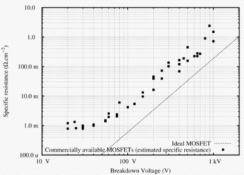
The power MOSFET is equivalent to the PIN diode, if it is in the OFF state and it is initiated by the P+ diffusion, the N- epitaxial layer and the N+ substrate. This structure is reverse biased when it is highly nonsymmetrical structure and the space charge region extends principally to the lightly doped side, which is the N- layers.
Even though, when the MOSFET is in the ON state, there is a no function of the N- layers. Moreover, it is lightly doped rejoin, intrinsic resistivity is non-negligible and it is added to the MOSFET ON- state drain to source resistance.
Break Down Voltage
There are two important parameters to run both the breakdown voltage and the RDSon of the transistor, which is the doping level and the thickness of the N- epitaxial layer. If the layer is thicker, it has low doping level and the breakdown voltage is high. Similarly, thicker the layer, it has the high doping level and the radon is low. Hence we can observe that there is a trade-off in the design of the MOSFET, between the voltage rating and the ON state resistance.
Body Diode
The body diode can be seen in the following figure that the source metallization is connected to both the N+ and P implantations. Even though the basic principle of the MOSFET requires only that the source should be connected to the N+ zone. Thus, this would result in a floating P zone between the N-doped source and drain. It is equivalent to an NPN transistor with a nonconnected base. Under some conditions like high drain current, in the order of the same volts of an on-state drain to source voltage, this parasitic transistor of NPN should be triggered and make the MOSFET uncontrollable.
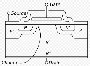
Body Diode
The connections of the P implantation to the source metallization short the base terminal of the transistor parasitic to its emitter and it prevents the latching. Hence this solution creates a diode between the cathode & anode of the MOSFET and the current blocks in one direction.
For inductive loads, the body diodes utilize the freewheeling diodes in the configuration of H Bridge & half bridge. Generally, these diodes will have a high forward voltage drop, the current is high. They are sufficient in many applications like reducing part count.
Working of Power MOSFET and Characteristics
The construction of the power MOSFET is in V-configurations, as we can see in the following figure. Thus the device is also called as the V-MOSFET or V-FET. The V- the shape of power MOSFET is cut to penetrate from the device surface is almost to the N+ substrate to the N+, P, and N – layers. The N+ layer is the heavily doped layer with a low resistive material and the N- layer is a lightly doped layer with the high resistance region.
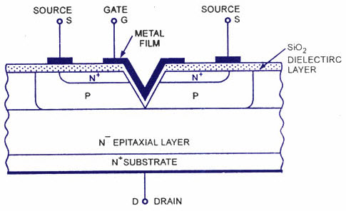
N – Channel Power MOSFET
Both the horizontal and the V cut surface are covered by the silicon dioxide dielectric layer and the insulated gate metal film is deposited on the SiO2 in the V shape. The source terminal contacts with the both N+ and P- layers through the SiO2 layer. The drain terminal of this device is N+.
The V-MOSFET is an E-mode FET and there is no exists of the channel in between the drain & source till the gate is positive with respect to the source. If we consider the gate is positive with respect to the source, then there is a formation of the N-type channel which is close to the gate and it is in the case of the E-MOSFET. In the case of E-MOSFET, the N-type channel provides the vertical path for the charge carriers. To flow between the drain and source terminals. If the VGS is zero or negative, then there is no channel of presence and the drain current is zero.
The following figures show the drain & transfer characteristics for the enhancement mode of N-channel power MOSFET is similar to the E-MOSFET. If there is an increase in the gate voltage then the channel resistance is reduced, therefore the drain current ID is increased. Hence the drain current ID is controlled by the gate voltage control. So that for a given level of VGS, ID is remaining constant through a wide range of VDS levels.
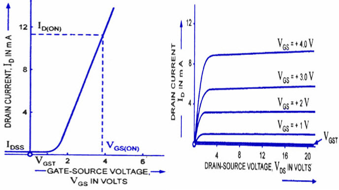
Transfer & Drain characteristics
The channel length of the power MOSFET is in the diffusion process, but in the MOSFET the channel length is in the dimensions of the photographic masks employed in the diffusion process. By controlling the doping density and diffusion time, the channel length will become shorter. The shorter channels will give, the more current densities which will contribute again to larger power dissipation. It also allows a larger transconductance gm to be attained in the V-FET.
In the geometry of power MOSFET, there is an important factor which is the presence of lightly doped, N- epitaxial layer which is close to the N+ substrate. If the VGS is at zero or negative, then the drain is positive with respect to the source and there is a reverse biased between the P- layer & N- layer. At the junction the depletion region penetrates into the N- layer, therefore it punch-through the drain to the source are avoided. Hence, relatively high VDS are applied without any danger of device breakdown.
In the power MOSFET, there is available of P-channel. The characteristics are similar to the N-channel MOSFET. The direction of the current and voltage polarities are in reverse direction.
Please refer to this link to know more about FET MCQs
MOSFET Power Amplifier
There are different types of MOSFET power amplifiers like 300W MOSFET power amplifier, 240W MOSFET power amplifier, 160W MOSFET power amplifier and 100W MOSFET power MOSFET amplifier. But here we are explaining about the 100W MOSFET power amplifier with its circuit.
100W MOSFET Power Amplifier Circuit Operation
The circuit operation of 100w MOSFET amplifier consists of PNP transistor from the differential amplifier circuit. The AC input signal is sent to one of the transistors and the other transistor gets the output signal from the feedback. The AC signal is a coupled to the base terminal of the transistor Q1 with the help of the coupling capacitor and the feedback signal. The feedback signal is fed into the base terminal of the second transistor Q2 with the help of resistor R5 & R6. The potentiometer is used to set the output of the amplifier.
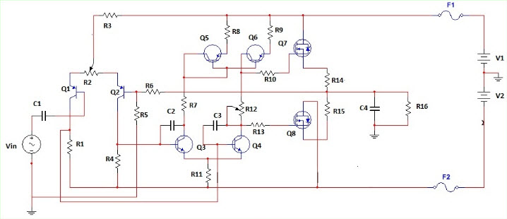
100W MOSFET Power Amplifier Circuit Operation
The first stage differential output amplifier is fed to the second stage differential amplifier input. In the case of the first differential amplifier, when the input voltage is more than the feedback voltage than the input voltage of the two transistors Q3 and Q4 of second differential amplifier differs from each other. The current mirror circuit of the transistors is Q5 & Q6. This circuit ensures the flowing of output current in the push-pull amplifier circuit is constant.
Thus, this circuit can be achieved because, when the collector current of transistor Q3 is increased, the collector current of Q4 decreases is to maintain the flow of constant current through the universal point of the emitter terminal of the transistors Q3 &Q4. There is an equal output current in between the current mirror circuit & collector current of the Q3 transistor. The potentiometer R12 protects the applications of DC biasing to each MOSFET because the two MOSFETs are in the balancing to each other.
If the positive voltage is applied to the gate terminal of the Q7 transistor then it will conduct. Correspondingly transistor Q8 will conduct for the negative threshold voltage. To prevent the MOSFET output from the oscillating the gate resistors are used.
Applications of Power MOSFET
The power MOSFET’s are used in the power supplies
- DC to DC converters
- Low voltage motor controllers
- These are widely used in the low voltage switches which are less than the 200V
This article will give the information on the working principle of power MOSFET circuit and its applications. We hope by reading this article you have gained some basic knowledge and understanding about the power MOSFET. Here is the question for you, what are the functions of the power MOSFET?