In the developmental era of semiconductor diodes itself, Zener diodes were founded. Every electronic circuit is basically composed of diodes. So, diodes hold utmost prominence in the development of electrical and electronic devices. The characteristics of Zener diode were initially described by Clarence Melvin Zener in the year 1934. From then, there has been enormous progress in the implementation of these devices. To know about Zener diodes, one has to know about semiconductors where because a diode is generally constructed of semiconductors. So, let’s dive into a discussion of the Zener diode circuit, its working principle, construction, applications, and advantages.
What is a Zener Diode?
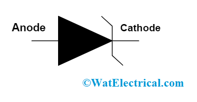
Zener diodes are also called as reference diodes because they hold the ability even to deliver constant reference voltage levels for most of the electronic circuits. In similar to semiconductor diodes, Zener diodes also have almost similar characteristics. In forward condition, the properties are the same as that of semiconductor and in reverse diode the operation is varied. For minimal voltage levels, there will be not much conduction whereas when the voltage level reaches a certain limit, there will be a breakdown and current flow exists. When the performance characteristics of the Zener diode circuit are considered, the voltage is constant in spite of current levels which means that the output of diode is a constant reference voltage for increased current values. The circuit symbol of this diode can be shown as

zener-diode-symbol
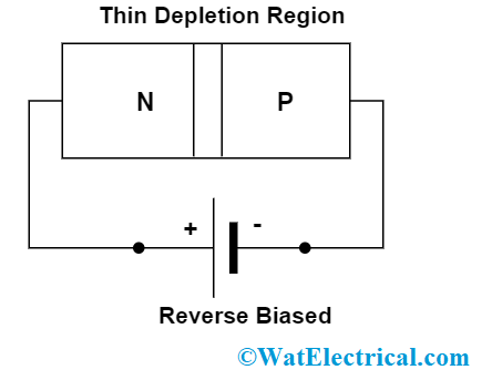
It has a specially doped depletion region which is aimed to conduct only in the reverse biased condition upon the reach of specified voltage level. Furthermore, voltage drop stays as constant for extended voltage levels where this characteristic allows diodes to be used in voltage regulations. Zener diode circuit diagram can be shown as follows.

zener-diode-circuit
The diode is operated in reverse bias condition which means that the diode’s n-type is connected to the positive edge of the power source and the p-type is connected to the negative edge of the power source. As because the diode is constructed with the semiconductor element, it has an extremely thin depletion region.
Zener Diode Working Principle
In the reverse biased condition, the diode’s depletion layer gets broad and upon enhancement of voltage levels, the layer extremely wider. At this point, there happens a steady reverse saturation current because of minority charge carriers. Here, the minority charge carriers gain energy because of the application of the electric field and when they crash with the static ions and release free electrons. The released electrons also gain energy and again develop electrons.
As there happens the situation of more electron’s creation, the depletion layer will be of more electrons and the Zener diode becomes completely conductive. This phenomenon corresponds to avalanche breakdown but shows no intense functionality. Whereas when the PN junction is doped extremely, the intensity of the atoms will be more. More atoms in the diode enhance the ions concentration and so the width of the depletion layer will become thin and this happens for the same reverse-biased voltage level as that of previous.
As because of the thin depletion layer, the electric field across this region is very high. After a reach of certain reverse-biased voltage, the electrons breakdown the covalent bonds and come out. This phenomenon corresponds to Zener breakdown. The voltage where this breakdown happens is considered as Zener voltage. When the supply voltage is greater than that of Vz, there happens a conductive path and no possibility of avalanche breakdown to take place.
Ideally, Vz takes place at minimal voltages mainly in the case of Zener breakdown. At the time of the manufacturing process, Zener voltage will be corrected through perfect doping levels.
Zener Diode Characteristics
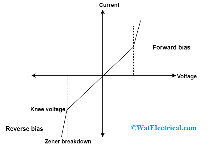
The characteristics, voltage, and breakdown levels are clearly understood through this graphical representation. The operation of the Zener diode illustrated in a graph is also termed as V-I characteristics of the diode.

v-i-characteristics
In forward bias condition, the diode operates in normal condition whereas in the reverse bias condition, when the reverse voltage is more than Vz, there happens Zener breakdown. So, in the picture, the voltage level ahead of Vz is the Zener voltage, also called knee voltage because here the current valve enhances quickly. The voltage flow through the diode is calculated by
V = Vz + IzRz
Applications
Zener diode is mostly employed in many manufacturing and business requirements. The following are the Zener diode applications.
Zener Diode as a Voltage Regulator
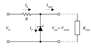
Here, the diode delivers constant voltage level to the output from the applied source whose voltage levels might differ over a range. It can be clearly known with the circuit diagram shown below:

voltage-regulator
Here, Vz is in parallel connection to the RL in the case of reverse bias. The voltage across the load resistance is Vz where this is the applied voltage (V0 = Vz). The variation in the output voltage is gripped by the resistor that is in series connection with that of the circuit. Through this connection, there will be a constant voltage level at the output.
When there is the application of a variable voltage at the RL and Vin is minimal to that of Vz, then there will be no current flow and so Vin = Vz. There will be a flow of more current when Vin>Vz, so that the series resistor R receives more current and this enhances the voltage drop across R.
When Vz voltage is connected in parallel to the load in that of reverse direction so that the load voltage is Vz and so there will be stabilization of the voltage at the output.
- Zener diodes are also used as multimeters to regulate the meter movement in any case of unintended excess loads. As it is in parallel connection with the diode, during excess load the excess current will be passed by the diode. So, this safeguards the meter from destructions and damages.
- These diodes are also utilized for the transmission of sine shaped signals to that of square signals. This is achieved by positioning two Zener diodes in series connection with that of R. These are back to back connected and in the reverse direction. When the applied voltage is minimal to that of Vz, then the diode will deliver an increased resistive path and similarly when Vin is more than Vz, then the diode will deliver minimal resistive path. As because of this, the increased voltage drop across sine wave and R is limited and the output will be a square wave.
FAQs
1). What is a Zener diode used for?
Zener diodes are mostly employed for the regulation of voltage levels.
2). What is the difference between a diode and a Zener diode?
A normal diode functions only in forward bias condition whereas Zener diode functions both in forward and reverse bias conditions.
3). Can Zener diode be used as a rectifier?
In comparison to that of normal diodes, Zener diodes are heavily doped and they can go through breakdown showing no destructions. So, utilized for rectification functions also.
4). Why Zener diode is not used in forwarding bias?
In forward bias, a normal diode can be used because both the diode operates similarly in forwarding bias.
5). Is a transistor a diode?
Yes, transistors are employed as diodes.
So, this is all about the concept of Zener diode and these diodes have multiple specifications and they might vary based on operating voltage level, reverse current flow, packaging and power dissipation. A few of the specifications to be considered for every diode are minimum and maximum levels of voltage and current, power rating, voltage tolerance point, Zener resistance, temperature stability, and package. So, know more about the varying properties and how Zener diode characteristics vary?