We all know that the basic passive linear elements in the domain of electrical and electronics are capacitor, resistor, and inductor. These elements are integrated to form various types of electric circuits. The major circuit types are RC, RLC, LC, and RL where these combinations exhibit major kinds of performance which are essential to analog electronics. In specific, they hold the ability to perform as passive type filters. In a practical way, capacitors are majorly chosen than inductors as the design of those is simple and easy.
Both the RL and RC type circuits can be created as a single-pole filter. Based on whether the ‘L’ or ‘C’ reactive element is in series or parallel connection with the load, the type of the filter can be known as low-pass or high-pass. This article mainly describes on RL circuit, its definition, differential equation, time constant, RL circuit differential equation, and other related concepts.
What is RL Circuit?
This circuit is also termed as RL filter or network where the RL circuit definition is stated as that it is an electric circuit that consists of the major elements resistor and inductor which are connected together those are powered by either current or voltage source. Because resistor exists in the circuit, the RL circuit will consume energy which is similar to RLC or RC circuits.
Below is the basic RL series circuit where the components inductor ‘L’ and resistor ‘R’ are in series connection with a supply voltage of ‘V’ volts. Assume that the current flow through the entire circuit is ‘I’ amperes and the flow of current through resistor and inductor is IR and IL correspondingly.
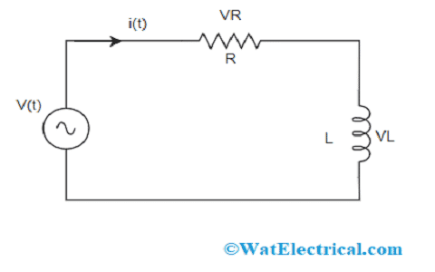
Basic RL Circuit
As the resistor and inductor components are in series connection, the current flow all across the circuit is the same which is
IR = IL = I
Based on Kirchhoff’s voltage law which defines that supply voltage equals the sum of the voltage across resistor and inductor. So,
V = VR + VL
RL Circuit Equation Derivation and Analysis
When the above shown RL series circuit is connected with a steady voltage source and a switch then it is given as below:
Consider that the switch is in an OPEN state until t= 0, and later it continues to be in a permanent CLOSED state by delivering a step response type of input. This initiates the current flow across the circuit in a steady manner but not reach its peak value ‘Imax’ as defined by the ratio of Ohm’s law which is V/R. This restraining factor is because of the existence of self-generated EMF.
This EMF is generation is because of the development of magnetic flux. Later on, after some period of time, the voltage counteracts this EMF where the current flow remains constant and induced current gets to ‘0’ value.
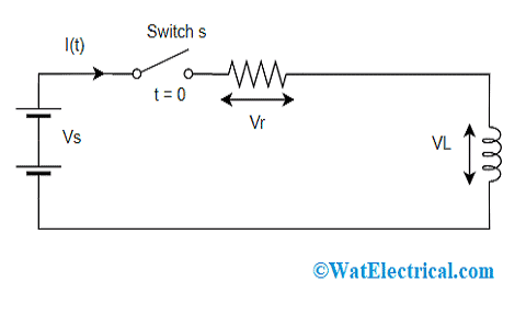
Series RL circuit
As discussed above, that
V = VR + VL
V- VR + VL = 0
The voltage drop across inductor and resistor is given by
VR = I × R and VL= L(di/dt)
So, the RL circuit formula is given by
V = I × R + VL= L(di/dt)
With the above equation, it can be stated that VR is based on the current ‘i’, whereas VL is based on the rate of change in current.
When the current value reaches ‘0’, then the above equation becomes first order RL circuit differential equation where this can be modified to provide current value at any time instant which is
I(t) = V/R [1- e-Rt/L] (A)
Here, ‘V’ is measured in volt
‘R’ is measured in ohm
‘L’ is measured in Henry
‘t’ is measured in the second
‘e’ = 2.718
The time constant of a series RL circuit is represented by L/R where V/R corresponds to the ultimate steady-state current which happens after 5 time steady values. When the current value reaches the peak steady-state which is at 5τ, then the coil’s inductance lessens to ‘0’and behaves like a short circuit. So, the current flow across the coil is restricted by the resistive component. The graph that depicts current v/s voltage/time attributes is featured as the transient response of the RL circuit.
Transient Response
As it was already discussed that
VR = I*R
The VR will have similar growth and shape exponentially like current, whereas VL consists of an exponential factor Ve-Rt/L. Then the voltage drop across ‘L’, possesses an initial value equals to the value of battery voltage at t = 0. Or else, V across ‘L’ will have a value when the switch is initially closed and then reduces to ‘0’ in an exponential way as shown in the below graphical curve. The transient time of the inductive circuit is known by its relationship with resistance.
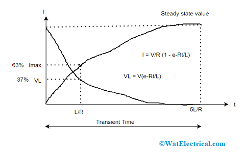
Transient Response
For instance, consider a resistor with a steady value of resistance. Here, the larger is the inductance value, the minimal is its transient time and so the time constant of the RL circuit is longer. In a similar way, to achieve a longer transient time, a steady inductance value has to be considered.
Though, for a steady value inductance when the resistance value and transient time are increased, then the time constant will gradually reduce. This happens because when the circuit’s resistance increases, the inductance value is minimal when compared with the resistance value which results in negligible transient time.
So, in an RL circuit when the frequency is increased
- The entire impedance of the circuit increases
- Phase angle increases
- Resistance value stays constant
- Inductive reactance increases as XL has a direct relation with frequency
Power Factor
In an RL series circuit, some amount of energy is dissipated by a resistor and some amount is consecutively accumulated and returned by an inductor where
- The immediate amount of power delivered by the voltage source is P = VI which is measured in watts.
- The amount of power dissipated by a resistor is P = I2R
- The amount of energy that is accumulated in the inductor is given by
P = VLI = LI (dI/dT)
So, the entire power factor of the RL circuit is given by the power dissipated by the resistor along with the power absorbed by the inductor
P = I2R + LI (dI/dT)
The power triangle is shown below
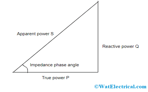
Power Triangle of RL Circuit
Phasor Diagram of RL Circuit
The phasor diagram of a series RL circuit is represented as below:
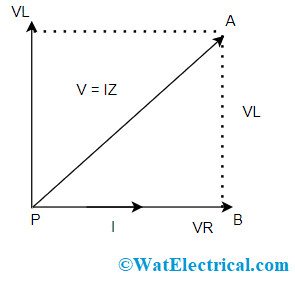
Phasor Diagram of RL Circuit
To draw a phasor diagram for the circuit, below are the steps to be followed
- Consider, the current ‘I’ as a reference point
- The voltage drop that takes place across resistor VR = IR is drawn in the exact phase with that of current ‘I’.
- Whereas the voltage drop that takes place across the inductive reactance VL = IXL is drawn in the above phase with that of current because of current lags voltage by an angle of 900 in the case of a purely inductive circuit.
- The supply voltage is then the sum of voltage drops across the resistor and inductor.
When we consider a right-angled triangle PAB as per the above diagram, then
V = √[(VR)2 + (VL)2]
√[(IR)2 + (IXL)2]
√I[(R)2 + (XL)2]
As we know that I = L = V/Z
Z = √[(R)2 + (XL)2]
Where ‘Z’ is the entire amount of opposition for the direction of alternating current and this is called as the impedance of the RL circuit.
The Impedance of RL Circuit
In this RL circuit, impedance contradicts the direction of alternating current. Here, impedance is defined as the combined impact of resistance and inductive reactance of the circuit. The impedance is shown by
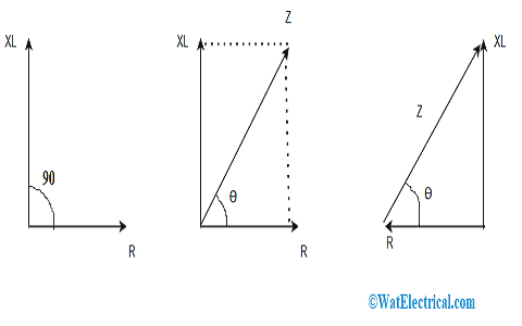
Impedance Response
Z = (R2+ XL2)0.5
In the case of a right-angled triangle, the phase angle value is given by ϴ = tan-1 (XL/R)
Consider the below pictures
Response Functions of RL Circuit
The impulse response of the RL circuit for each voltage is considered as the inverse Laplace transform of a specific transfer function. This characterizes the circuit’s response to an input voltage which includes an impulse.
For an inductor voltage, the impulse response is given by:
hL(t) = δ(t) – [R/L(e-t(R/L)u(t)]
- δ(t) – 1/τ (e-t/τ u(t)
Here, u(t) is Heaviside step function and τ is the time constant represented by L/R
In the same way, for a resistor voltage, the impulse response is
hR(t) = R/L(e-t(R/L)u(t)] = 1/τ (e-t/τ u(t)
The natural response of an RL circuit is termed as zero input response where this response defines the circuit’s performance when it reaches constant voltage and current values. At this condition, the circuit gets disconnected from the power source. This is called ZIR as there is a null power source.
The natural response of this circuit is given by
I(t) = I(0) e-t(R/L) = I(0) e-t/τ
RL Parallel Circuit
The prominence and usage of a parallel RL circuit are less when compared with a series RL circuit if not it is driven by a current source. It is not much considered because Vout equals Vin which means that the circuit does not hold the ability to function as a filter for supply voltage.
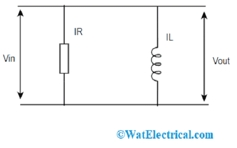
Parallel RL Circuit
In consideration of complex impedances,
IR = Vin/R
IL = Vin/jωL = jVin/ωL
As per the above equation, the inductor lags the resistor by an angle of 900. The parallel circuit is observed as the output of multiple amplifier circuits as it insulates the amplifier from the capacitive loading impacts at higher frequency levels. As because of the phase shift effect by capacitance, few amplifiers tend to be unstable and oscillate which shows the impact on sound quality.
Uses
The RL circuit uses consist of the following:
- These are mainly used in RF amplifiers
- Implemented for the purpose of signal processing and filtering of circuits
- Used in oscillator circuits
- Employed in variable tune circuits and radio wave transmission systems
- Utilized as DC power supplies in the RF amplifiers
- Used for the magnification of voltage and current values.
Know More about Capacitors in Series.
Know More about Single Phase AC Circuits MCQs, Alternating Current and Voltage MCQs.
This is the overview of an RL circuit. This article has provided a detailed analysis of RL circuit definition, derivation, power factor, impedance response, its formulas, circuit diagram, and uses. In addition, know what is the step response of the RL circuit and how does it impact the circuit’s performance?